Our approach
We understand that reliability is paramount
Crystalaid offers a full spectrum of testing and inspection services. Our engineers design and deploy custom test jigs tailored to your needs and conduct thorough testing to ensure adherence to design specifications. Our specialised testing validates product integrity, simulates the impact of real word usage, and aids in crafting user manuals. Our experienced in-house test engineering team can lead the whole process, or are available to provide additional support to your team. We ensure seamless execution from start to finish.
Automated Optical Inspection
Accurate defect detection
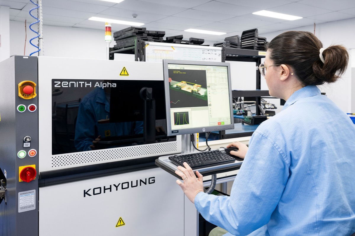
Our AOI systems, equipped with advanced optics and image processing capabilities, are integral in identifying defects at high-speed manufacturing rates. Whether utilising 2D or the more sophisticated 3D AOI technology, we ensure meticulous inspection of components, capturing defects that traditional methods might miss. This real-time feedback mechanism enhances overall production quality, aligning with the rapid pace of Surface Mount Technology (SMT) lines.
Functional Testing
Optimal PCB performance
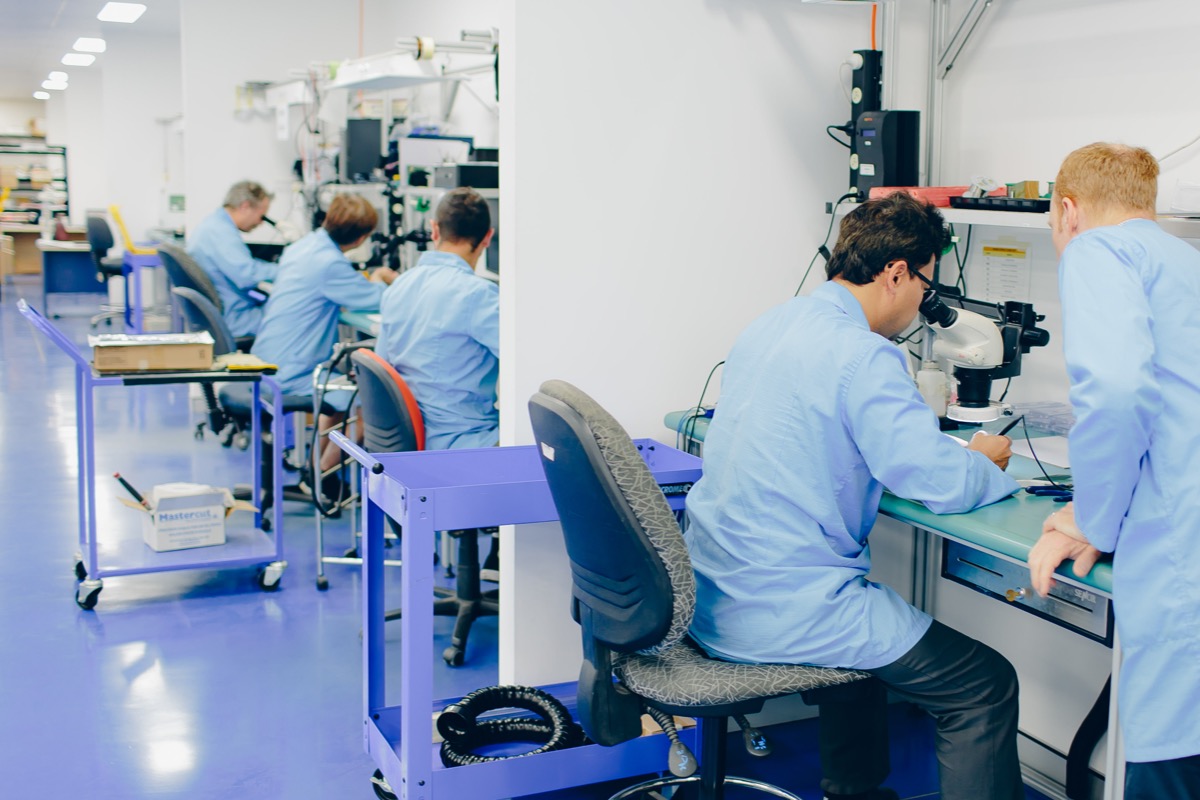
Functional Testing at Crystalaid involves a thorough evaluation of your PCB’s behaviour under simulated operational environments. By applying various signals and currents, we verify each component’s functionality, ensuring your PCB performs exactly as intended. This meticulous process significantly reduces the likelihood of defects and failures, offering you a product that’s reliable and robust.
Flying Probe Testing
Flexible PCB analysis
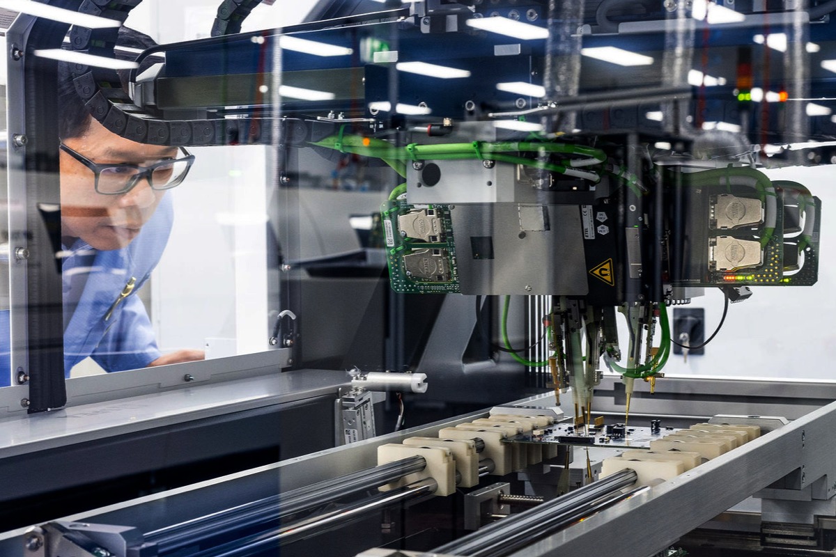
Flying Probe Testing offers a versatile approach to PCB inspection, especially suitable for low-volume runs. Using robotic test probes, this method measures key electronic properties without power application, providing both in-circuit and functional test capabilities. The flexibility of not requiring custom fixtures makes Flying Probe Testing an ideal choice for quick, efficient, and accurate PCB testing.
Thermal Cycle Testing
Enhanced product durability
Thermal Cycle Testing at Crystalaid assesses the durability of materials under temperature extremes. This testing is critical in identifying potential issues like solder joint cracking and warping. By simulating years of field installation conditions, we ensure that your products withstand the rigours of real-world use, maintaining their functionality and integrity.
X-Ray Inspection
Comprehensive solder joint analysis
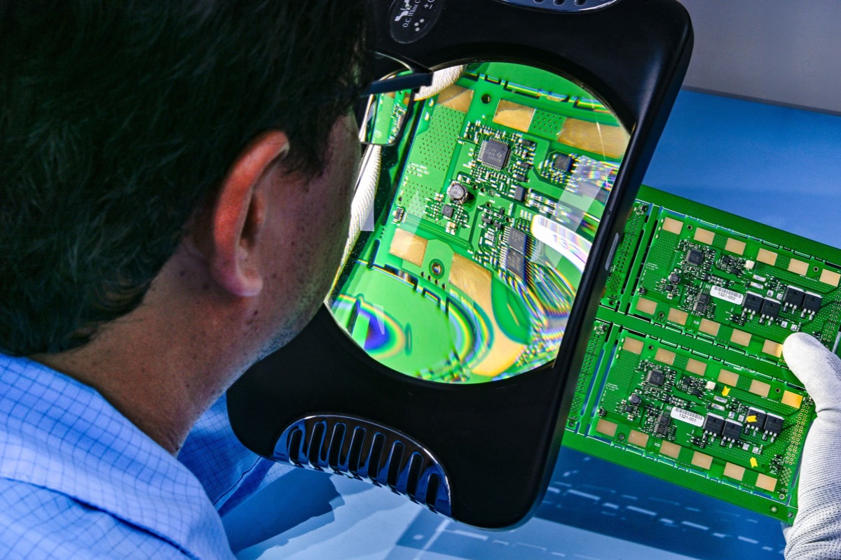
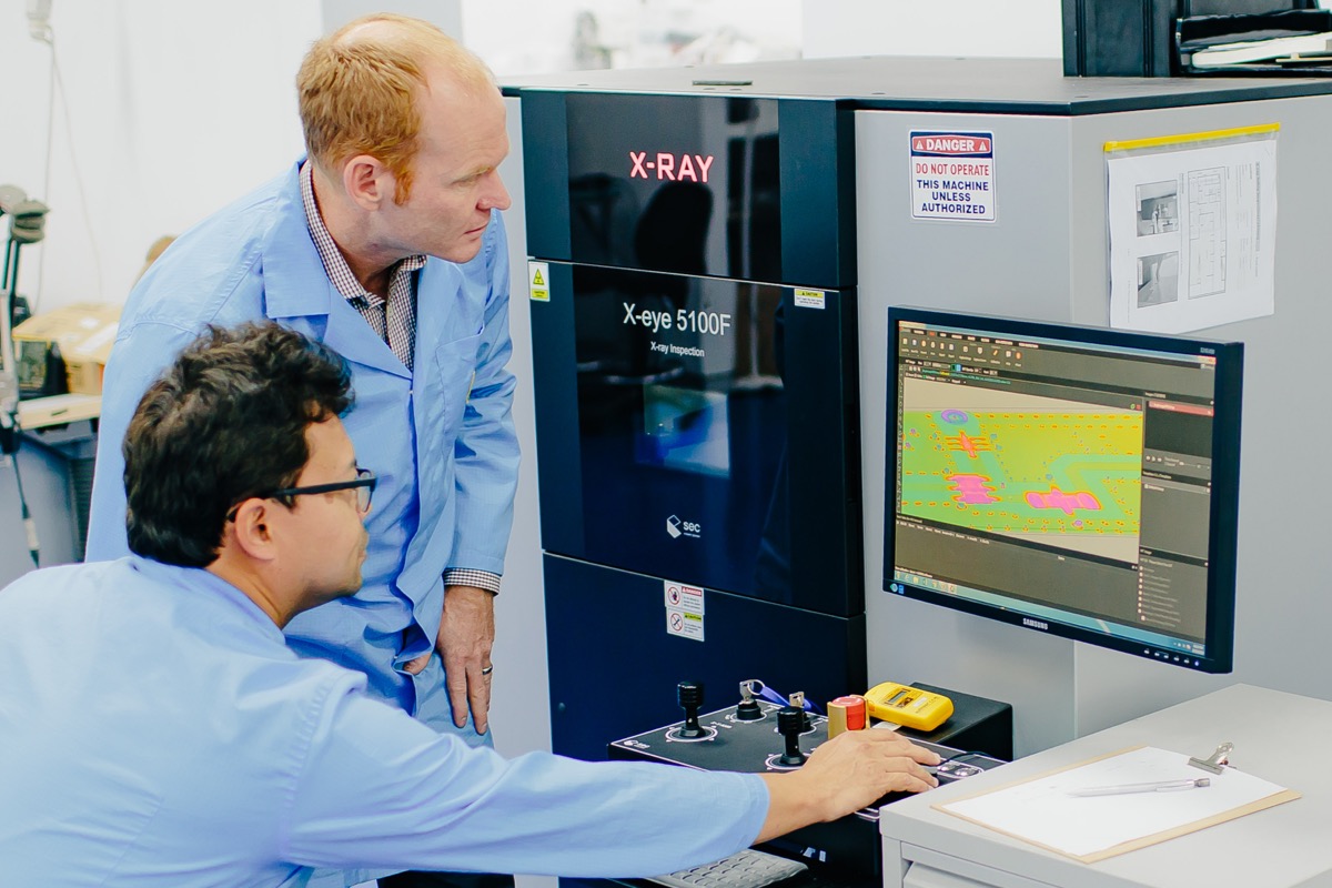
Our X-Ray inspection service complements our AOI capabilities by providing an in-depth view of solder connections, including those hidden beneath components like BGAs. This non-invasive inspection method ensures thorough validation of all solder joints, guaranteeing the structural integrity and reliability of your assembled PCBs.
FAQ’s
Thermal Cycle Testing exposes your products to extremes of temperature, identifying any potential issues related to material durability. This ensures that your products are reliable and can withstand real-world environmental conditions.
Our X-Ray inspection can identify a range of defects, especially in solder joints, including those underneath BGAs. This method is essential for ensuring the overall quality and structural integrity of your PCB assemblies
Yes, we are equipped to handle testing for high-volume electronic products. Our testing methodologies, including AOI and Functional Testing, are designed to keep up with the demands of high-speed manufacturing.
Flying Probe Testing is particularly beneficial for low-volume or varied PCB assemblies. It offers the flexibility of testing without custom fixtures, and its robotic probes provide precise measurement of electronic properties.